
The $5 Billion Push to Accelerate Innovation - Six Five Connected with Diana Blass
SHARE


On Connected, Diana Blass tours Applied Materials' $5 billion EPIC Center, where chipmakers, equipment developers, and researchers will work in parallel to move AI chip breakthroughs from lab to market faster. Earlier collaboration could cut years from development cycles as AI demand outpaces manufacturing capacity.
Can chipmaking move fast enough for AI when a single materials breakthrough can take 10 to 15 years to reach a commercial chip? Demand for AI compute is already growing faster than new manufacturing capacity can come online, and chips are getting more complex with every generation: more three-dimensional, built from multiple dies, and connected through advanced packaging. A change in one part of the chip now ripples through everything else, which makes the industry's traditional step-by-step development process a bottleneck.
Diana Blass goes inside Applied Materials' $5 billion EPIC Center, on this episode of Six Five Connected. She explores the new R&D facility in Silicon Valley designed to fundamentally change how semiconductor technologies are developed and commercialized. Featuring insights from Applied Materials President and CEO Gary Dickerson, alongside Mukund Srinivasan, Tristan Holtam, Sundeep Bajikar, Adam Brand, and Kelly Truman, with an industry analyst perspective from Daniel Newman, the episode explores a new approach to semiconductor R&D.
EPIC is designed to run research, equipment development, process integration, and commercialization in parallel, giving customers access to new technologies years earlier than a traditional pilot-line handoff allows. Moor Insights & Strategy's Patrick Moorhead has estimated the approach could cut development timelines by roughly 30%, and some of the first projects target one of the industry's biggest bottlenecks: 3D DRAM.
Key Moments:
🔹 AI demand is outrunning manufacturing capacity. New fabs take years to bring online, and the companies shaping chip requirements now include Google, Amazon, and Tesla alongside traditional semiconductor makers.
🔹 Materials engineering is where the next gains come from. Applied works with layers just a nanometer or two thick, controlled to within an angstrom, as logic, memory, and advanced packaging all move toward 3D and multi-die designs.
🔹 Sequential development no longer keeps pace. Taking a breakthrough from material science to high-volume manufacturing can take 10 to 15 years, and defining each new node now requires more people solving more interconnected problems together.
🔹 EPIC puts the ecosystem under one roof. Announced in May 2023, the facility includes more than 175,000 square feet of advanced cleanroom space, about four acres, and is expected to bring together more than 1,000 researchers and technologists, including students.
🔹 Earlier access can cut years from development. Customers can work with new technologies before they reach pilot-line maturity, with early projects focused on the bottlenecks standing between the industry and 3D DRAM.
🔹 Universities extend the frontier. University research explores materials beyond what's in manufacturing today, such as next-generation conductor materials, which Applied can then scale up to 300-millimeter wafers.
Chipmakers that bring equipment, materials, and research partners into development earlier will be best positioned to deliver the next generation of AI chips on time.
Watch the full video at sixfivemedia.com, and subscribe to our YouTube channel so you never miss an episode.
Learn more about Applied Materials at appliedmaterials.com.
Disclaimer: Six Five Media is for information and entertainment purposes only. Over the course of this video, we may discuss companies that are publicly traded, and we may reference their equity share prices. Nothing discussed during this webcast should be considered investment advice or a recommendation to buy or sell any security. We are not investment advisors, and you should not rely on this content as financial advice. Six Five Media collaborates with technology companies and industry leaders to produce research-driven interviews and multimedia programming for enterprise technology audiences.
Diana Blass:
Chips have been at the center of the A.I. boom. They sit inside the servers powering A.I. where they process and move enormous amounts of data at incredible speeds. But A.I.
Mukund Srinivasan:
Demand is growing faster than the manufacturing capacity that is coming online.
Diana Blass:
Long before the A.I. boom, semiconductors powered everything from smartphones and computers to cars and data centers. Decades of innovation didn't just make chips more powerful, it made massive amounts of computing power cheap enough to scale.
Gary Dickerson:
Your smartphone that has tens of billions of transistors, 60 miles of wiring, and it costs $30. I mean, you think about what we've been able to create in this industry. It is a miracle.
Diana Blass:
And now AI is demanding the next miracle. One that requires chips to deliver far more power, consume far less energy, and reach market much faster.
Tristan Holtam:
From coming up with a breakthrough in material science, moving that through product development, and integrating it into a high-volume manufacturing environment in a commercial chip, that process can take 10 or 15 years.
Diana Blass:
The pressure point is the process itself. As chips become more complex, the technologies inside them have to become incredibly interconnected.
Daniel Newman:
Individual manufacturers can no longer carry the entire load.
Diana Blass:
So we came here.
Tristan Holtam:
So this is where many of those chipmaking technologies will be born.
Diana Blass:
It's called EPIC, a $5 billion R&D center in Silicon Valley created by Applied Materials. The company develops the equipment and manufacturing technologies chipmakers use to build advanced semiconductors.
Daniel Newman:
They feel the optimism to spend big and bet big because this is going to be big.
Diana Blass:
We first visited Epic in July of 2026, when it was still under construction.
Diana Blass:
It's in a fitting location here in Silicon Valley, home to Intel, Apple, and countless semiconductor pioneers.
Diana Blass:
But increasingly, the companies shaping the future of chips extend well beyond the traditional semiconductor industry.
Sundeep Bajikar:
Like Google, like Amazon, like Tesla.
Diana Blass:
It all speaks to an exploding demand for AI compute, one Applied Materials anticipated when it announced Epic in May 2023.
Tristan Holtam:
So the core concept of EPIC is can you execute the technology roadmap faster? Can you innovate and commercialize next generation technology faster? And that speed, that velocity comes from tighter collaboration.
Diana Blass:
The reason goes back to a shift applied Spotted years ago. One that would change not just how much compute was needed, but how that compute had to be built for AI.
Sundeep Bajikar:
Just running software on general purpose processors, which had been the model for a long time, would no longer be adequate.
Diana Blass:
Applied works at the materials level. It's focused on the building blocks inside a chip, what they're made of, how they're structured and how they connect. That gives the company a close view into how logic, memory and advanced packaging are all evolving.
Gary Dickerson:
So you think about advanced logic to process data. Some of these materials that we're creating They're a nanometer or two nanometers thick, and you need to control to within an angstrom, which is a tenth of a nanometer, a millionth the size of the human hair, and we're just bringing all of this materials innovation together to enable that computing innovation.
Tristan Holtam:
As we look to the future, what we're seeing is that chips and chipmaking technology continue to grow in complexity. So the dimensions of the chip continue to shrink. The features in the chip are becoming more and more three-dimensional. And we're moving from monolithic silicon, where you would have a single chip on a single piece of silicon, into an era of multi-die chips that are then connected together using advanced packaging technology.
Diana Blass:
That creates new ways to pack more capability into a system, but it also means a change in one part can ripple through everything else.
Sundeep Bajikar:
It takes a lot more people that have to solve a much more complex problem to define the next node and the node after that.
Tristan Holtam:
And this is why working more closely with our partners and our customers, working more closely than ever before is so important. And Epic is going to be a big part of that way of working.
Diana Blass:
You can see how much of these halls are still taking shape.
Diana Blass:
The plan, though, was to fill them with engineers, researchers, and chip makers.
Daniel Newman:
You're bringing leaders of innovation from Korea, from Japan, from Taiwan, of course here in America, and they're all coming into one facility, working on shortening those timelines, delivering value sooner.
Diana Blass:
And this is a look at where all of that work will take place. The facility includes more than 175,000 square feet of advanced clean room space, about four acres, and is expected to eventually bring together more than a thousand researchers and technologists, including students.
Kelly Truman:
We also find the universities have a lot of capability we don't have, right? They're on cutting edge beyond what's already in manufacturing. So we do find, oh, wow, that's really cool. We, you know, this next class of conductor materials, we'll say this looks like the best one and we'll bring it back and put it up to 300 millimeter. So there's a lot of great stuff like that happening at the universities.
Diana Blass:
And that's the broader idea behind EPIC. bring research, equipment development, process integration and commercialization closer together, so more of the work can happen in parallel instead of one step at a time. And analysts expect that it will pay off. Patrick Moorhead of Moore Insights and Strategy has estimated that approach could cut development timelines by roughly 30 percent. And speed matters when some of the industry's biggest bottlenecks are already here, like memory.
Adam Brand:
3D DRAMs is the best idea in the industry right now of how to deliver really a major step forward. We're doing projects with our customers in the Epic Center. They're going to address some of the key bottlenecks that have to be solved in order to make the 3DDRAM technology possible.
Tristan Holtam:
Traditionally, we would need to wait for that technology to reach a level of maturity where it was possible to ship a prototype system into a customer pilot line. With Epic, we can provide customers with much earlier access to those new technologies that are being developed, and that can cut years from their development cycle.
Diana Blass:
And that timing matters. The U.S. is in the middle of a massive semiconductor buildout, with hundreds of billions of dollars going into new fabs and R&D, driven not only by AI, but growing demand across automotive, communications, and other industries, along with a push for a more resilient chip supply chain. But more fabs are only part of the equation. Those factories still need the equipment, materials, and manufacturing processes capable of producing the next generation of chips.
Gary Dickerson: This inflection will determine who wins and loses around the world and in every single market and every single industry. And so the compute demand is gonna keep going up.
Diana Blass:
So while the future of Epic remains to be seen, one thing we did see on our tour today is that the future of innovation doesn't just have to do with the chips, but the manufacturing technologies behind them. It'll be fascinating to see what happens next, so be sure to stay tuned. I'm Diana Blass, and now you're connected to the story behind AI.
MORE VIDEOS

What It Takes for AI Agents to Earn the Right to Act
Snowflake’s Pavan Pothukuchi explains why enterprise AI agents still struggle to act on systems of record, and how governed data platforms, semantic layers, and scoped agent identity close the gap. For enterprise leaders, agent autonomy has become a data architecture decision.


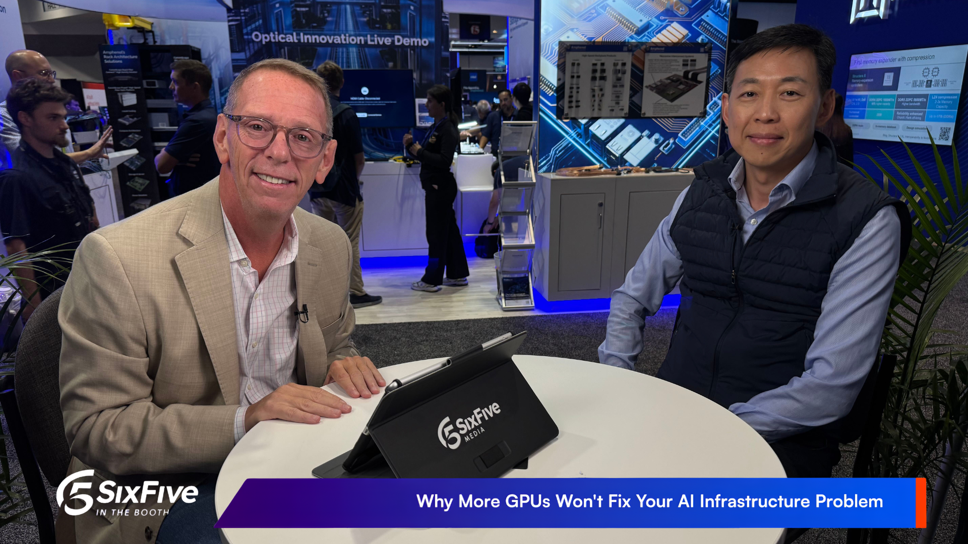
Why More GPUs Won't Fix Your AI Infrastructure Problem
At OCP Global Summit 2026, MiTAC Computing's Raymond Huang explains why AI infrastructure has become a full-stack integration problem spanning compute density, cooling, firmware, and deployment speed. For data center operators, advanced cooling and open management are now as decisive to scaling AI as GPU selection.
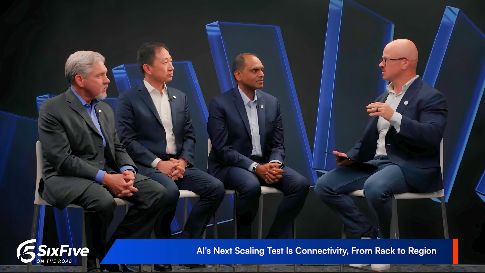
AI’s Next Scaling Test Is Connectivity, From Rack to Region
Marvell’s Sandeep Bharathi, Xi Wang, and Russ Esmacher explain why connectivity has become AI’s next rate limiter, from the copper wall inside the rack to scale-across links between AI clusters. For hyperscalers, the connectivity bets made today must hold up across multiple bandwidth generations.
Other Categories
CYBERSECURITY

Threat Intelligence: Insights on Cybersecurity from Secureworks
Alex Rose from Secureworks joins Shira Rubinoff on the Cybersphere to share his insights on the critical role of threat intelligence in modern cybersecurity efforts, underscoring the importance of proactive, intelligence-driven defense mechanisms.

HP Launches World’s First Business PCs to Protect Against Quantum Hacks - The Six Five On the Road
On this episode of the Six Five - On the Road, hosts Patrick Moorhead and Daniel Newman are joined by HP's Ian Pratt, Global Head of Security for Personal Systems.

What is Autonomous Endpoint Management?
Autonomous Endpoint Management is a framework designed to unify IT operations and security teams on a single platform through real-time control and visibility.
QUANTUM
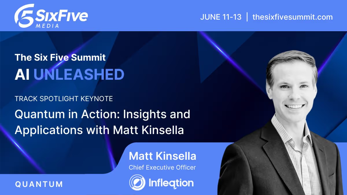
Quantum in Action: Insights and Applications with Matt Kinsella
Quantum is no longer a technology of the future; the quantum opportunity is here now. During this keynote conversation, Infleqtion CEO, Matt Kinsella will explore the latest quantum developments and how organizations can best leverage quantum to their advantage.
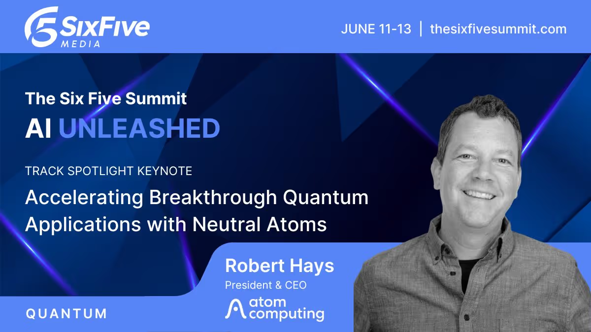
Accelerating Breakthrough Quantum Applications with Neutral Atoms
Our planet needs major breakthroughs for a more sustainable future and quantum computing promises to provide a path to new solutions in a variety of industry segments. This talk will explore what it takes for quantum computers to be able to solve these significant computational challenges, and will show that the timeline to addressing valuable applications may be sooner than previously thought.